- Home
- Scanning Acoustic Microscope (SAM/SAT)
Scanning Acoustic Microscope (SAM/SAT)
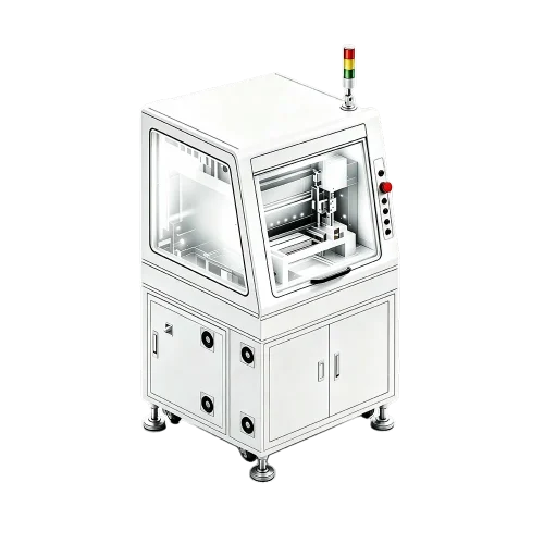
The Scanning Acoustic Microscope (SAM/SAT) enables the high-resolution, non-destructive testing of components and material structures using high-frequency ultrasound. The method is particularly suitable for the investigation of semiconductors, power electronics, and electronic packages where internal structures and defects must be analyzed without disassembly.
The ultrasound examination makes it possible to detect, among other things, delaminations, voids, cracks, and other abnormalities at material boundaries and connection points. The detected ultrasound signals are digitally processed and displayed as high-resolution images, allowing for targeted analysis of the position, size, and distribution of internal defects.
Working principle
The Scanning Acoustic Microscope works with high-frequency ultrasound and a liquid coupling medium, usually water. The test head sends ultrasound pulses into the component and receives the signals reflected off material boundaries and defects.
The received signals are analyzed and visualized in various representations:
A-Scan: Representation of the received ultrasound signals along the sound propagation time
B-scan: Two-dimensional representation of a selected section
C-Scan: Surface-based representation of a defined component plane
Depending on the test task, different scanning and evaluation methods can be used. This allows for the non-destructive localization and analysis of internal structures, interfaces, and defects.
Advantages of the SAM/SAT test
Non-Destructive Testing of Components and Assemblies
High-resolution imaging of internal structures
Detection of Delaminations and Voids
Analysis of Material Boundaries and Joints
Inspection without disassembling the component
Precise Localization and Analysis of Internal Defects
Suitable for research, development, process validation, and quality control
Typical applications
Power Semiconductors
IGBT Modules • SiC Power Modules • Power Modules • DBC Substrates • Power Devices
Semiconductor Packaging
Chip Packages • IC Packages • Flip-Chip Packages • MEMS • Ceramic Substrates
Other Applications
Delamination Testing • Void and Pore Analysis • Bond Joint Testing • Weld Defect Testing •
Inspection of water-cooled cooling plates • Examination of internal material defects • Thickness measurement of selected materials