
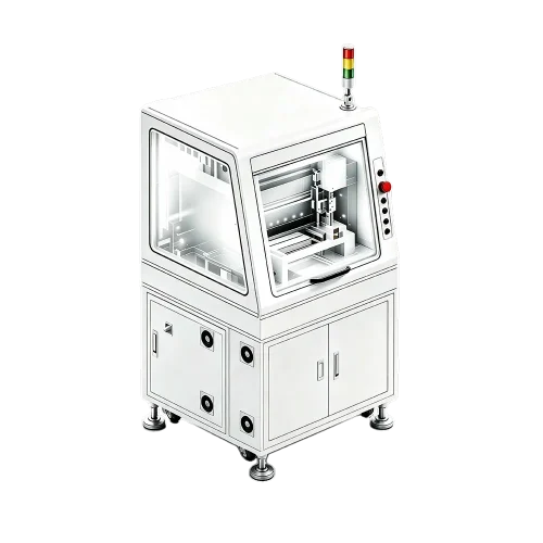
Non-destructive ultrasonic testing for semiconductors and technical components
The ultrasound examination enables the non-destructive examination of components and material structures. High-frequency ultrasound allows the detection of internal structures, material boundaries, and defects that are not visible from the outside.
Our ultrasound testing systems are particularly suitable for testing Semiconductors, power electronics, electronic packages, ceramic substrates, and water-cooled components.
Depending on the test task, different test heads, frequencies, and scanning methods can be used. This allows internal defects to be located, analyzed, and represented in a visual way.
Inspection of housings, bond and material layers for delaminations and defects
Inspection of seam connections, solder joints, and thermally stressed areas
Detection of detachments, voids, and structural irregularities
Investigation of internal structures and material connections
Non-destructive analysis of sensitive multilayer structures
Control of connections and interfaces within the package
Examination of internal structures, gaps, and possible manufacturing defects
We use cookies to improve your browsing experience, serve personalized ads or content, and analyze our traffic. By clicking „Accept All“, you consent to our use of cookies. For more information, please see our Cookie Policy.